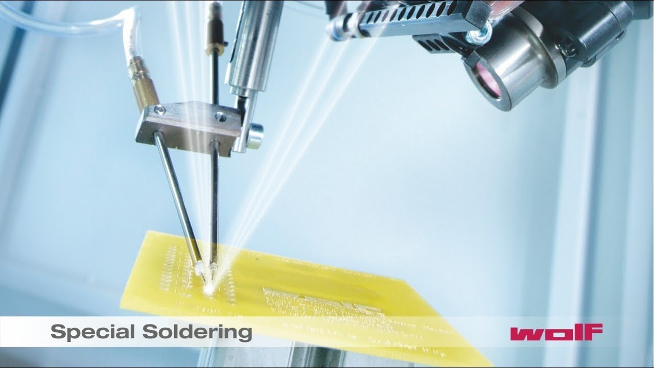
Lift/dip soldering is derived from dip soldering, which was used at the beginning of electronics production as a preliminary stage to wave soldering. While the entire PCB is soldered in conventional wave and dip soldering, only defined areas should come into contact with solder in selective soldering.
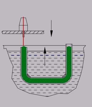
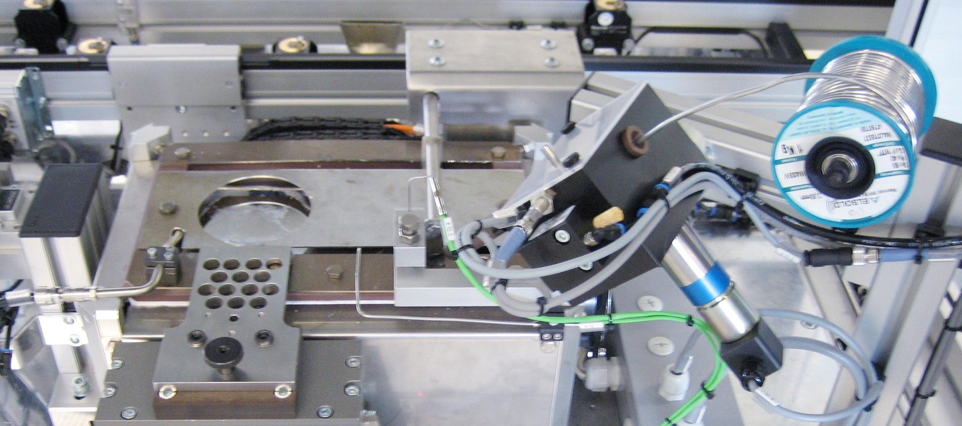
The workpiece is lowered onto the solder nozzles, on which there is a “solder deposit” with a convex surface (drop shape). To ensure a constant solder deposit, the principle of “communicating tubes” is used in the nozzle design. This means that the size and shape of the solder deposit is completely independent of the solder level of the solder bath. However, other parameters, such as the speed at which the solder is ejected from the solder bath, also play a role. The bath surface must be absolutely clean and oxide-free before the nozzles are immersed. The immersion of the nozzles and the lowering of the circuit board must be coordinated in a short time in order to avoid oxidation on the solder deposit surface and cooling of the solder deposit. The immersion depth has a major influence on the soldering quality. This must be kept constant and requires stable and precise machine mechanics.
Selective soldering systems can be set up as fully automatic machines in “in-line design” or as manual workstations. The basis is the Wolf standard cell.
We provide support in process development and offer the possibility of soldering tests and pre-series production in our technology center.
Application
Wired components still need to be soldered into SMD-equipped PCBs. Lift/dip soldering is particularly suitable if the solder joints are distributed across the PCB. This method only requires a free space of 1.5 mm around the soldering area. Nozzles with a minimum diameter of 5 mm are possible. Thanks to quick-change nozzle sets, the process can be used flexibly for a wide variety of solder joints.
The lift/dip soldering process is particularly suitable for tinning stranded copper wires and stripping enameled wires. Here, particularly high temperatures of up to 400°C are often required to melt off the enamel. The operation of mini-shafts is problematic at these temperatures.